Semiconductor-weize Semiconductor-weizeSemiconductor-weize

English
  • 简体中文
  • English
  • Home
  • about us
  • product
    • Semiconductor
    • Photomasks Field
    • Photolithography Field
    • Etching field
    • Thin Film Deposition & Metallization Field
    • Grinding Field
    • Measurement & Testing Field
    • Semiconductor

      • Photomasks Field

      • Photolithography Field

      • Etching field

      • Thin Film Deposition & Metallization Field

      • Grinding Field

      • Measurement & Testing Field

  • Agents brands
  • contact
  • 简体中文
  • English
Semiconductor
  • Semiconductor
Photomasks Field
  • Photomasks Field
  • Photolithography Field
  • Etching field
  • Thin Film Deposition & Metallization Field
  • Grinding Field
  • Measurement & Testing Field

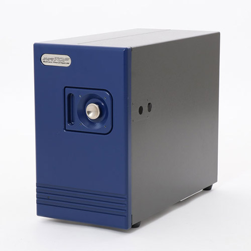
high-resolution time-of-flight mass spectrometer

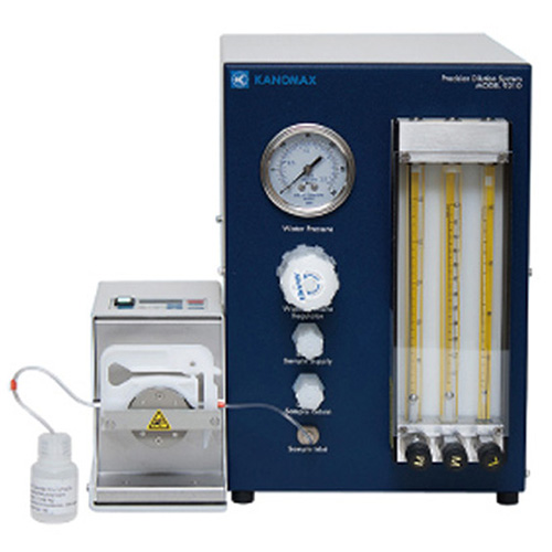
Precision dilution system_MODEL9210

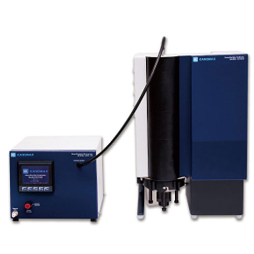
High efficient sampling system for nanoparticles_MODEL 9410

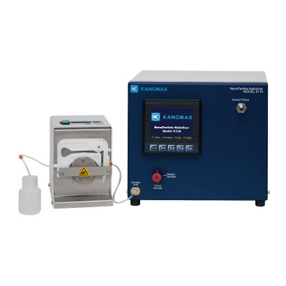
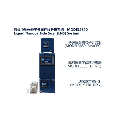
Nanoparticle atomizer_MODEL9110

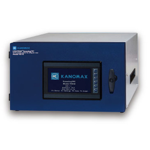
scanning type liquid nanoparticle counter_STPC3

liquid nanoparticle distribution online analyzer_LNS

  • Page 4 of 4
  • Home Page
  • 1
  • 2
  • 3
  • 4
  • Last Page
+86-021-58478283 Address:Address: Room 330, F-SPACE, Jinqiao Center, No.198 Leyuan Road, Pudong New Area, Shanghai, China Mobile:+86-18702113116 Email:helen@weizetech.com george@weizetech.com
扫描二维码

Scan the phone to add WeChat

Friend Link
  • 君点科技

Copyright © 2025 2018.Weize All rights reserved  Websitemap ICP:沪ICP备18038951号