Measurement & Testing Field-weize Measurement & Testing Field-weizeMeasurement & Testing Field-weize

English
  • 简体中文
  • English
  • Home
  • about us
  • product
    • Semiconductor
    • Photomasks Field
    • Photolithography Field
    • Etching field
    • Thin Film Deposition & Metallization Field
    • Grinding Field
    • Measurement & Testing Field
    • Semiconductor

      • Photomasks Field

      • Photolithography Field

      • Etching field

      • Thin Film Deposition & Metallization Field

      • Grinding Field

      • Measurement & Testing Field

  • Agents brands
  • contact
  • 简体中文
  • English
Semiconductor
  • Semiconductor
Measurement & Testing Field
  • Photomasks Field
  • Photolithography Field
  • Etching field
  • Thin Film Deposition & Metallization Field
  • Grinding Field
  • Measurement & Testing Field

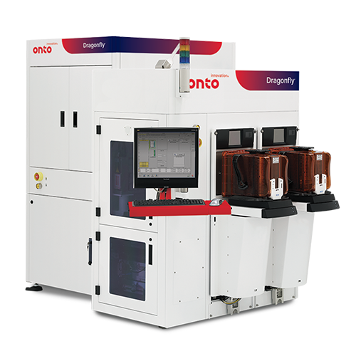
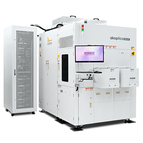
Advanced Wafer Inspection & Metrology System_Dragonfly G3

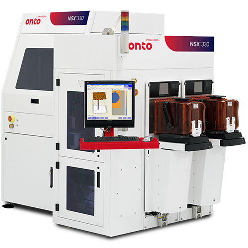
Advanced Wafer Inspection & Metrology System_NSX330

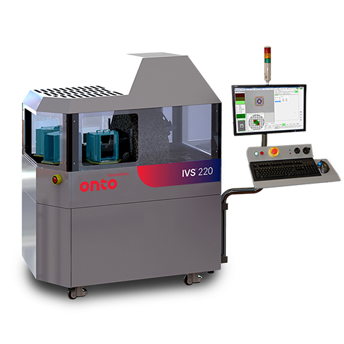
Optical Overlay & CD Metrology System_IVS220

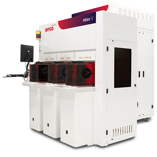
Advanced OCD & Thin Film Metrology System_Atlas

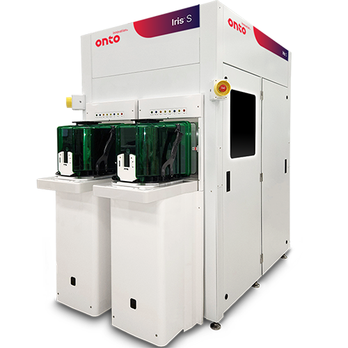
Advanced OCD & Thin Film Metrology System_IRIS S

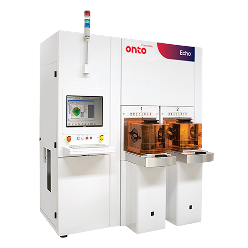
Advanced Metal Metrology with PULSE Technology System_Echo

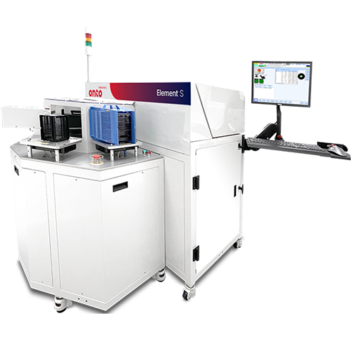
FTIR Metrology_Element S

CD-SEM_Gacii-SE046A

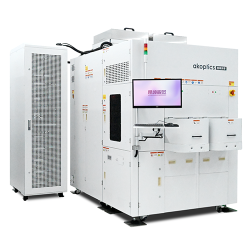
GaAsGaNInPLNLT substrate and epitaxial wafer defect detection equipment_E1000

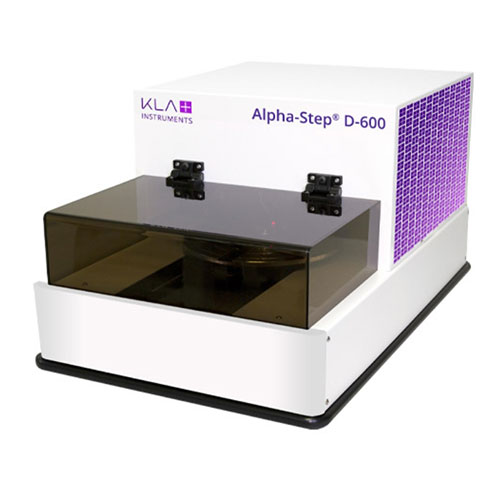
Stylus Profilometer 2D3D Stylus Measurement Alpha Step_D-600

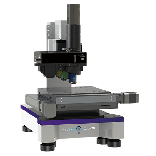
Optical Profiler_Zeta-20

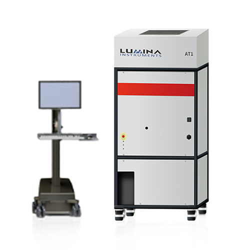
Defect Scanner_AT1AT2

SiC defect detection equipment_E3500
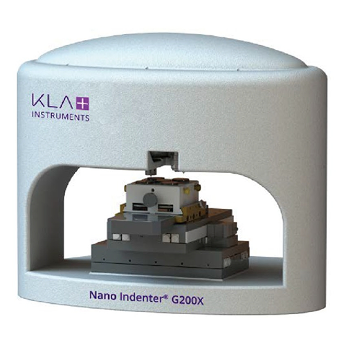
Nano Indenter_G200X

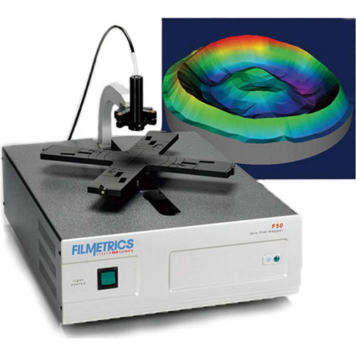
Thickness Measurement Mapping Instrument_F50

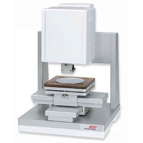
Sheet Resistance Mapping System_R50

  • Page 1 of 2
  • Home Page
  • 1
  • 2
  • Last Page
+86-021-58478283 Address:Address: Room 330, F-SPACE, Jinqiao Center, No.198 Leyuan Road, Pudong New Area, Shanghai, China Mobile:+86-18702113116 Email:helen@weizetech.com george@weizetech.com
扫描二维码

Scan the phone to add WeChat

Friend Link
  • 君点科技

Copyright © 2025 2018.Weize All rights reserved  Websitemap ICP:沪ICP备18038951号